-
Descripció
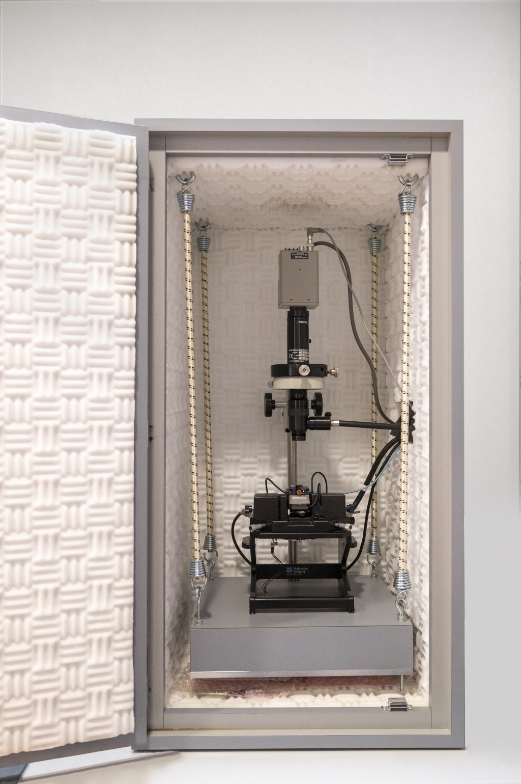
This technique is useful to easily elaborate three dimensional topographic maps of all kind of materials at nanometric resolution, through the surface of the sample, and atomic resolution (STM mode), along the perpendicular direction with respect to the sample's surface. Characteristic parameters of the surface roughness, layer thickness (from thin film depositions by sputtering), nanoparticles size or defects on the sample can be obtained by data processing.
The atomic force microscope Agilent 5500 can perform measurements in intermittent contact mode (tapping mode) and in contact mode, with the possibility to work in air or liquid (this application is important for biological samples). Electrical conductivity measurements can be performed on conductive samples (using a conductive tip). Also, maps of the magnetic domains distribution can be obtained by means of a magnetic tip.
The AFM operation is based on the detection of tiny atomic or molecular iteration forces between the tip and the surface of the material.
- Measurement of topography by contact mode
- Measurement of topography by the acoustic mode (tapping) for all type of materials: insulators, conductors, organics, etc.
- Phase measurements (composition contrast for different materials)
- Friction measurements
- Electrical force measurements
- Surface potential measurements (Kelvin probe)
- Magnetic force measurements
- Measurements of topography in liquids (dynamic studies on biological samples)
- Environmental chamber for inert atmosphere measurements
- STM (scanning tunneling microscope)
- Resistance measurements (by means of Resiscope II)
- Nanohardness and Young modulus measurements
- Nanolitography
-
Contact those
responsibles - Mariana Stefanova Stankova, Ph.D.
- 977558123
- mariana.stefanova(ELIMINAR)@urv.cat
- Dr. Eric Pedrol Ripoll, Ph.D.
- 977558473
- eric.pedrol(ELIMINAR)@urv.cat
-
Coordinadora tècnica
- Mercè Moncusí Mercadé
- 977558123
- merce.moncusi(ELIMINAR)@urv.cat
*Already registered on the User Portal?